
The Intel engine has started to purr. The company turned in a great quarter, and now CEO Bob Swan tells investors the Intel Xe DG1 GPU has been powered on in the lab.

Intel released their third-quarter results (see Intel Q3 2019 results) and reported record results. In the analyst call, Intel’s CEO Bob Swan said the company is on target to return to a schedule of major manufacturing upgrades every 2 to 2.5 years. In addition, Swan said, “We are on track to launch our first 7-nanometer-based product—a datacenter-focused discrete GPU—in 2021, two years after the launch of [a] 10 nanometer [version]. We are also well down the engineering path on 5 nanometer.”
Swan told investors that Intel has powered on the Intel Xe DG1 graphics AIB for the first time in the lab. Later in the day, Chris Hook celebrated this milestone with a tweet, “It’s alive!”
Hook maintains, via Twitter, that a ship date of 2020 is the schedule.
“Powered on,” means the initial testing has been accomplished in Intel’s labs and is in the process of validation. When final validation is completed, the Xe-based DG1 can move on to the next phase, which could (should) include external testing by potential OEMs and ODMs. When that happens, you can expect to see a torrent of leaks, and ferreted out discoveries about the highly anticipated chip.
We have received a smuggled photograph of the new card.
Robert Y. Kringly, an advisor and confidant to Intel, was able to visit the Intel Labs in Folsom and see some of the first generation testing and take a few pictures.
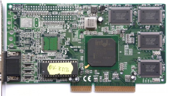
“Having worked with Roget Kadari and Kris Hooker when they were at AND,” Kringly told us through his thick Hungarian accent, “and all the Folsom Lab folks I was given special access to this amazing new card Intel will launch on February 1st, 2020 at CES.”
“It’s a little difficult to see the labeling on the chip,” Kringly added, “that is on purpose like the tiger striping automobile companies use when road testing a new car to throw off the paparazzi. Nonetheless, if you look closely you can clearly see the designation.”
The chip itself, we were told, has 4.6 billion transistors and is fabricated in Samsung’s 7-nm fab in Hwaseong, Korea. “The Intel engineers were a little embarrassed that the prototype couldn’t be made in their own fabs, but everyone knows why,” the Hungarian consultant added.
There are a cool 5,000 32-bit full floating-point shaders organized in 64 shader CUs, with independent texture engineers and a cross-bar interprocessor switching network buffered by 64mb caches. The 192-bit 10 Tbyte/s memory bus drives 64MB of 3DRAM (also from Samsung) and the tests Kringly saw showed the card delivering 25.5 TFLOPS. Remarkably, it did that in less than 110 W.
Mind you, none of this is verifiable. Repeated calls, faxes, and emails to Intel have so far not been answered, although a dead skunk did mysteriously show up in front of our door a few days ago.