The last five years have been an incredible roller coaster ride for AMD, the largest rival to Intel in the personal computer CPU marketplace. Jon Peddie takes a close look at both the company and their new Accelerated Processor Units.
By Jon Peddie
AMD has launched the latest in their alphabet soup of Fusion processors which they call APUs—accelerated processor units. AMD’s APUs are in fact HPUs — heterogeneous processor units with multi-core x86 CISC CPUs and many core SIMD GPUs. There are many remarkable aspects to these HPUs, not the least of which is their range of price, performance, power, and process.

Process prowess
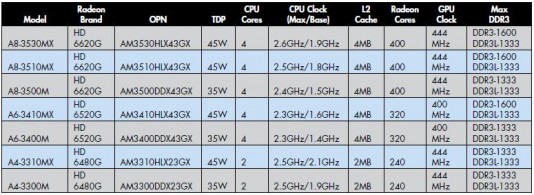
The specification differences speak for themselves (see Chart 1). What struck me was the fact that AMD has done something no other company has done before. They have brought X86 and GPU together in a merchant bulk CMOS process (40nm) using their chip manufacturer TSMC. And they recently announced a similar x86 and GPU integrated device in SOI HKMG (high-k/metal gate) at their other major chip manufacturing partner GlobalFoundries (32 nm). This is remarkable because it is a HKMG GPU implementation, and one of the few bulk CMOS x86 implementations, both examples made doubly complex and challenging by the integration of cache, GPU and x86. It also gives AMD an unusual dual-source capability for its range of HPU products.
The HPUs span a wide range of performance, power, price, and size categories such that AMD can truly say they have a device for every PC segment, right down to the darling tablets. The A8 offering of 400 GPU cores takes them to the entry level of workstations and HPU servers—that’s one heck of a span, and one that’s going to cause Intel and Nvidia some heartburn.
They call me Trinity, Z
AMD chose the recent Computex show in Taipei to set the stage, with more details to come at their developer conference in Seattle next week. At Computex, AMD unveiled its plans to produce a Bulldozer-based APU, codenamed Trinity, in 2012. The company also launched its Z-series chips, aimed at Windows tablets, and announced the official “A-Series APU” branding for its Llano series.
Also at Computex, Chris Cloran, AMD’s Corporate VP & GM of Products, said people had been asking “where AMD stood in their tablet approach.” He said it’s the Brazos-based Z-Series, with Desna chips that are set to show up this year followed by the Hondo line in 2012. These future chips will accelerate the next generation of applications, which are increasingly based on HTML5, Silverlight 5 and Flash 10.2x, and have a sub-6w TDP rating. They will be optimized for Windows, according to Cloran, and will provide the same experience “on a full tablet or clam shell.”
And with the expected floating-point capability in Bulldozer and the many-core GPU design, it is a safe bet that Trinity will be a gaming and media powerhouse next year. However, since the Z series will have a 6w TDP, which is more than Intel’s sub 3w Moorestown, or ARM-based processors with even sub 1w, it seems logical that the Z series will be AMD’s Windows engine for tablets and other portable devices and not an Android-based machine.

A… new APU series
The big, and more immediate news however, was the official roll-out of the A-series Llano HPUs from AMD, and what a line-up it is.
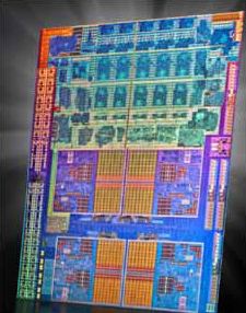
AMD has a nice slide (not reproduced here) that shows a Northbridge chip at 66 mm2 and 13 w, a quad-core CPU at 200 mm2 and 45 w, a GPU at 108 mm2 and 26.3 w being duplicated by an AMD APU at 228 mm2 and 35-45 w. Within that 228 mm2 die lurks more than a billion 32nm HKMG transistors (see die photo at beginning of story). And the combined performance of the A-series HPU is squeezing out about 500 GFLOPS.
C, E, and G
In addition to the A and Z series, AMD has the C, E, and G series, targeted at the Tablet and Netbooks, Ultramobile and Thin and Light notebooks, and the Embedded markets, respectively. The A series is for the mainstream Notebook, All-in-One, Desktop, and the Z series will be aimed at “HD” tablets.
The A series APU’s GPU is an updated version of the “Redwood” design; which has AMD’s talented UVD3 video engine, power gating, and a redesigned memory interface; and as mentioned earlier, the first DirectX 11 GPU to be made in 32 nm HKMG SOI process. The GPU has AMD’s new TeraScale 2 Unified Processing Architecture with tessellation, Shader Model 5.0, DirectCompute, and OpenGL 4.1 capabilities. It offers up to 24x MSAA, SSAA, and MLAA, and 16x angle-independent anisotropic filtering. AMD APP technology enables applications to take advantage of massive parallel processing via OpenCL 1.1. AMD A Series APUs also features additional enhancements that make the designs more developer friendly in tasks like moving data between CPU & GPU processing and memory.
AMD may be on the way to offering the universal video codec capability I and others long for with their third generation of UVD, as shown in the diagram. Depending upon the series number (A2, 4, 8, etc.) the CPU can have up to four cores and 4MB of L2 cache. AMD claims the inter-processor caching can result in more than 6% improvement from previous x86 generation cores, and the A-series CPUs have Turbo Core.
AMD has developed OpenCL-based stabilization software which AMD is branding as Steady Video. It’s included in their driver suite for the A-series. Steady Video uses the GPU for computational aspects of the stabilization. This is an AMD capability; the company also offers MotionDSP optimizations as a separate, standalone application. Steady Video is based on the AMD graphics/compute driver.
The A-series also has the ability to use the embedded GPU with an external GPU in AMD’s CrossFire mode which will be called “dual Radeon graphics.” AMD also has a switched graphics function (like Nvidia’s Optimus or Lucid’s Virtu) that allows the smaller of the two GPUs to run when on battery power and engage the bigger GPU when an application calls for it.
Hi ho hi ho, it’s off to market we go
AMD has re-labeled and branded the Fusion processors to cover all the PC segments from sub-$400 to -$700 and above, and taken a clear and direct aim at Intel’s line-up. AMD has improved their marketing mojo considerably and the company is taking an in-your-face stance with Intel. AMD is bragging about having sold (shipped) over 5 million of the Brazos E- and C-series HPUs, and expects to do even better with the A-series.
AMD’s target is to ship one million notebook-use Llano APUs in June, 1.5 million in July, and a total of from 8 million to 9 million for the whole of 2011. Acer recently placed an order for 80,000 units. AMD also took home the Best Choice of Computex Taipei award.
What do we think?
AMD has truly built a supercomputer chip for notebooks. With a quad-core x86 CPU and Turbo-core, and up to 400 GPU cores, the compute horsepower in this tiny low-power chip is astounding.
It has taken AMD five years from the time it announced the acquisition of ATI and the plan to offer Fusion processors to deliver the Llano. In the process the company shed its fab, won a settlement with Intel, fired two presidents, and dramatically repositioned the company and brand. I can’t think of any other company that has done so much and changed so much in five years and lived to tell about it. Not only lived to tell about it, but AMD has gotten bigger and better in the process. Fusion has reshaped the industry, and moved it in AMD’s favor. That’s one helluva accomplishment.
Dr. Jon Peddie is president of Jon Peddie Research. This article originally appeared in TechWatch, a JPR publication.


