Samsung announces plans to scale the mountain.
Do you know why airplanes that weigh more than the air they displace can fly? It’s because everyone on board believes it is possible. Every time someone on a flight reasons out that an airplane, or a bee, can’t fly, airplanes and bees fall out of the sky. It’s a fact, look it up—do the research.
 Did you know you have really fat hair? I’m talking about the diameter of human hair. Fatter than the color red or IR, for that matter. A single strand of hair equals 1,000,000 Ångströms. A million of them. Samsung is going to build a transistor gate so small that 714,285 of them could fit in the cross section of your fat hair. Imagine what you could do with hundreds of thousands of transistors in your hair—I can’t.
Did you know that the emperor not only has new clothes, but that airplanes and bees can fly, and that Samsung can make transistors so tiny that if you ate 300 million of them, they wouldn’t be larger than the salt on your hamburger?
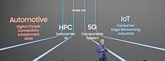
At its annual Samsung Foundry Forum event, Dr. Siyoung Choi, president of the foundry, said that significant market growth in high-performance computing AI, 5/6G connectivity, and automotive applications has created demand for advanced semiconductors—and the demand has increased dramatically. That makes innovation in semiconductor process technology critical to the business success of foundry customers. To that end, Samsung highlighted its plans for advanced process technology.
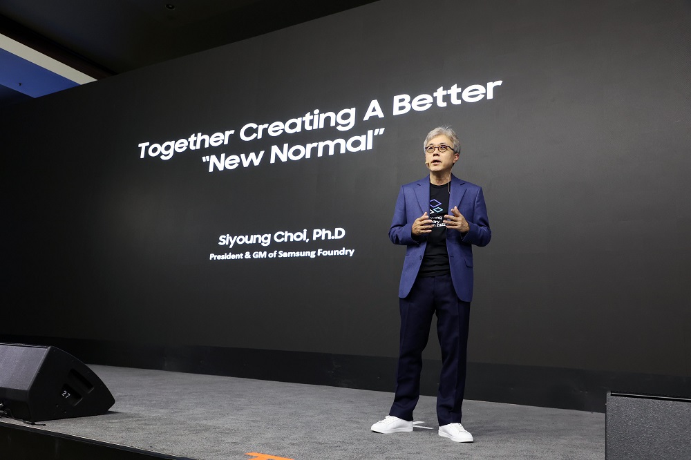
“The technology development goal down to 1.4 nm and foundry platforms specialized for each application, together with stable supply through consistent investment, are all part of Samsung’s strategies to secure customers’ trust and support their success,” said Choi. “Realizing every customer’s innovations with our partners has been at the core of our foundry service.”
With the company’s success of bringing 3 nm process technology to mass production, Choi said Samsung will be further enhancing its gate-all-around (GAA)-based technology and introducing a 2 nm process in 2025 and a 1.4 nm process in 2027.
Choi said Samsung is also accelerating the development of 2.5D/3D heterogeneous integration packaging technology to provide a total system solution in foundry services.
Through continuous innovation, its 3D packaging X-Cube with micro-bump interconnection will be ready for mass production in 2024, and bump-less X-Cube will be available in 2026.
The company plans to target high-performance and low-power semiconductor markets such as HPC, automotive, 5G, and the Internet of Things (IoT).
During 2022, Samsung introduced customized and tailored process nodes. Choi said the company will enhance its GAA-based 3 nm process support for HPC and mobile, while further diversifying the 4 nm process specialized for HPC and automotive applications.
For automotive, Samsung is providing embedded non-volatile memory (eNVM) based on 28 nm technology. In order to support automotive-grade reliability, the company plans to further expand process nodes by launching 14 nm eNVM solutions in 2024 and adding 8 nm eNVM in the future. Samsung has also been mass-producing 8nm RF following 14 nm RF, and 5nm RF is currently in development.
In addition to 70 partner presentations, Samsung Design Platform teams will introduce the possibility of applying Samsung’s processes such as Design Technology Co-Optimization for GAA and 2.5D/3DIC.
As of 2022, Samsung provided over 4,000 IPs with 56 partners, and is also cooperating with nine and 22 partners in the design solution and EDA, respectively. It also offers cloud services with nine partners and packaging services with 10 partners.
Along with its ecosystem partners, Samsung provides integrated services that support solutions from IC design to 2.5D/3D packages.