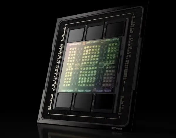
According to Korea’s The Elec, Nvidia is seeking to diversify its sourcing of high bandwidth memory (HBM3) and 2.5D packages, according to sources familiar with the matter. The company is in talks with potential suppliers, including Samsung, to secure alternative options for these critical components.
Currently, Nvidia relies on TSMC (Taiwan semiconductor manufacturing company) for the front-end process of manufacturing the wafers and 2.5D package work for its A100, H100, and other AI GPUs. However, due to the increasing workload associated with the 2.5D packaging, TSMC is facing capacity constraints.
To address this challenge, Nvidia is exploring partnerships with secondary suppliers, such as Amkor Technology from the US and SPIL (Siliconware precision industries Ltd) from Taiwan. Meanwhile, SK Hynix will continue to exclusively supply the HBM3 chips used by Nvidia.
Samsung’s advanced package team (AVP) has emerged as another potential supplier for Nvidia. The AVP team, established by the South Korean tech giant in late 2022, aims to expand revenue from chip packaging. Samsung has proposed a collaboration where it would receive Nvidia’s AI GPU wafers from TSMC and procure HBM3 from its memory chip business unit. Samsung would then utilize its own I-Cube 2.5D packaging technology to complete the manufacturing process.
Samsung’s proposition includes committing a substantial number of engineers to the project and offering to design the interpose wafer for Nvidia. Sources suggest that if the deal goes through, Samsung could handle around 10% of Nvidia’s AI GPU package volume.
However, before finalizing the agreement, Samsung needs to meet Nvidia’s requirements and successfully pass quality tests for its HBM3 and 2.5D package. Samsung is targeting the start of HBM3 production later this year and expects it to contribute to the company’s chip division profits from next year onward.
Meanwhile, TSMC is also planning to increase its 2.5D packaging capacity by over 40% to meet the growing demand from Nvidia. This suggests that if Samsung fails to meet Nvidia’s evaluation criteria in a timely manner, it may lose the opportunity to secure the deal.
Samsung is additionally focusing on the development of a bump-less package, known as Cu to Cu, direct bonding, or hybrid bonding, by 2025. This technology aims to reduce package height and is particularly suitable for high-layer HBM.


