In the face of soaring global demand for graphics processing units (GPUs), Nvidia, the leading player in the AI-focused GPU market, has turned to Taiwan Semiconductor Manufacturing Company (TSMC) and its advanced packaging technology, CoWoS. Meanwhile, Samsung is gearing up to challenge TSMC’s packaging prowess, signaling an imminent packaging rivalry between the two tech giants.
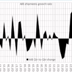
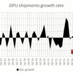
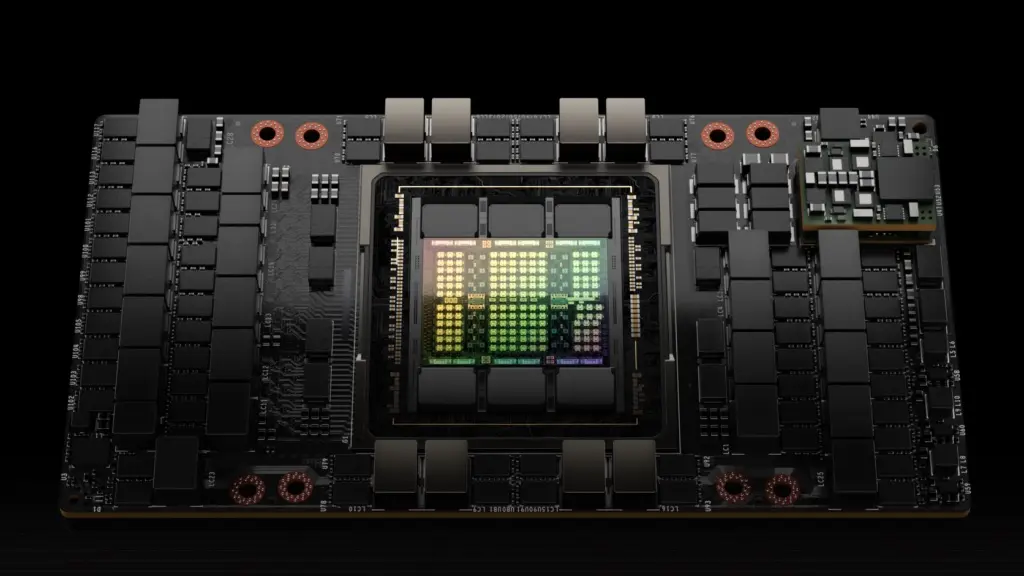
Nvidia’s GPUs, such as the renowned A100 and H100 models crucial for AI programs, are entirely outsourced to TSMC. However, the tight supply of GPUs has driven prices to unprecedented levels, prompting Nvidia to collaborate with TSMC to scale up packaging capacity. TSMC’s exclusive ability to deploy Nvidia chips stems from its highly regarded packaging technology, CoWoS.
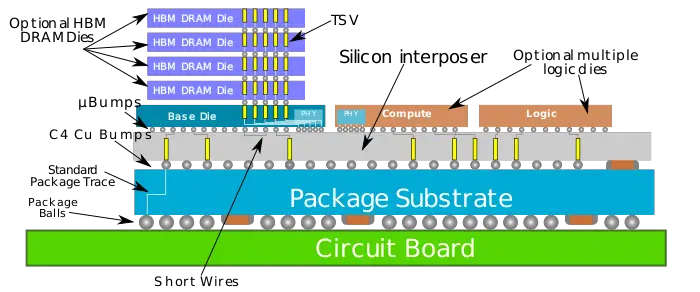
The packaging process involves stacking chips in a three-dimensional arrangement within a thin film, resulting in reduced distances between them and faster chip-to-chip connections. This technique yields substantial performance gains, surpassing 50 percent in some cases. TSMC introduced CoWoS technology in 2012 and has continually upgraded its packaging capabilities. This expertise has made TSMC a vital partner for Nvidia, Apple, and AMD, as their core products heavily rely on TSMC’s packaging solutions.
While Nvidia and other industry giants remain loyal to TSMC, Samsung Electronics has set its sights on challenging TSMC’s packaging dominance. Samsung, which had earlier achieved the mass production of 3-nanometer semiconductors ahead of TSMC, unveiled its ambitious plans at the Samsung Foundry Forum 2023 for Korea, which was reported on by local news services. According to Business Korea, the company aims to advance its packaging technology, develop a robust ecosystem, and offer customized packaging services to enhance chip performance. Samsung envisions a dedicated packaging line and is actively developing advanced packaging concepts like I-cube and X-cube technologies, with a particular focus on three-dimensional (3D) chip stacking.
The stage is set for a head-to-head competition between Samsung and TSMC in the packaging realm, with Samsung’s drive to excel in this field matching TSMC’s renowned CoWoS technology. As the global semiconductor industry acknowledges the critical role of packaging in chip performance, Nvidia’s partnership with TSMC solidifies the latter’s market position as a leading packaging specialist. At the same time, Samsung’s relentless efforts to develop advanced packaging technologies position it as a formidable challenger to TSMC’s packaging dominance.