Jon Peddie says the totally new GPU architecture based on 28nm technology is a home run.
By Jon Peddie
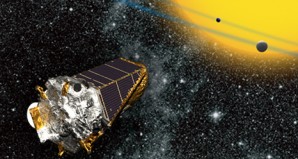
The NASA spacecraft Kepler was named after 17th century mathematician, astronomer, and astrologer Johannes Kepler. And Nvidia has chosen to name their newest processor after both of them. Streams of data are coming from outer space as the Kepler spacecraft carries on its mission in search of Earth-size and smaller planets around other stars. So far it’s found 61 confirmed planets and 2,321 planet candidates.
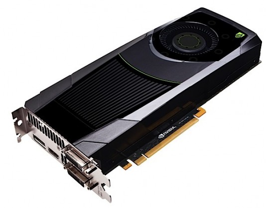
NASA computes must sort through reams and reams of data to find the tiny perturbations indicating a planet. Life will be easier for NASA now that the 28nm 1GHz 1,536-core Kepler GK104 is available from Nvidia.
Just as the Keplers that came before it, Nvidia’s Kepler broke the mold. A totally new architectural design, exploiting the benefits of tiny 28nm technology to gain big performance with little use of power—this is one of the best designs Nvidia has done (the TNT and G80 would be the other bests).
Was Fermi a test platform?
When Nvidia introduced Fermi we could see it was a different machine; although it borrowed from previous designs. It ran hot, but it had some novel concepts not the least of which was the Shader Multiprocessor (SM) design which is the heart of the machine. In the GK104 there is a brand new SM and a lot of them. Nvidia calls the new processor the SMX and the X can be appreciated if you compare the GK104 to the previous Fermi GF104.
Kepler’s new architecture provides a dramatic increase in the number of unique textures available to the shaders, and that allows different materials and richer textures in a scene. Prior to Kepler if a GPU needed a texture, it had to be assigned a “slot” in a fixed-size binding table. How many unique textures a shader can read from at run time was limited to 128 slots in Fermi (which aligned with the API limits of DX11).
Kepler introduced bindless textures so the shader can reference textures directly in memory, making binding tables obsolete. Eliminating the limits on the number of unique textures that can be used to render a scene means over 1 million unique textures are possible. Besides dramatically increasing the number of available textures, another added benefit of bindless textures is reduced CPU utilization:
Getting ahead of the puck
One of the advantages a designer gets with a clean sheet of paper is the opportunity to shed a lot of accumulated stuff and start anew. That’s the good news. The scary part is when you design a supercomputer in 294 mm2 of silicon that is going to go into production five years from the time you begin, you better guess right about where the industry, technology, software, and associated parts like memory are going to be—the ultimate “be where the puck is going to be” test. We think Nvidia got it right, better than right—this is an out-of-the-park home run design.
Nvidia claims that the underlying changes made to its SMX architecture result in a theoretical doubling of performance per watt compared to Fermi. We and others will be testing the new Kepler to see if the chip and its AIB implementations live up to the promise, but our feeling is that we won’t be disappointed.
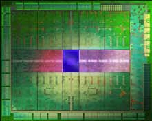
Nvidia did several clever things in Kepler resulting in a chip that has 18% more transistors (3.54 billion) in a die size that is 44% smaller, while increasing the GPU clock 30%. You just can’t do that kind of stuff by simply turning dials on a simulator and going to a smaller process, you’ve got to have a totally new approach. Graphics lives and dies on its memory performance and speed. Here again Kepler is a leap forward, cranking up the GDDR5 clock 50% to 1.5 GHz. Normally that would work the memory manger so hard it would melt, so there’s another view of the elephant that indicates what a new design this is. The net result is the memory bandwidth, although staying basically the same, lifts the texture fill rate 260% to a mind-boggling 128.8 GTEX/s.
The layout of the chip, which is so dense it looks like abstract art, nonetheless shows the organizational structure of the device. It’s easy to see from the layout how the part could be de-populated and used for say, well, how about a mobile part? Read on.
Nvidia also added core power balancing, similar to what Intel calls turbo; Nvidia calls it GPU boost. In cases where the GPU isn’t fully taxed, it would be useful if the GPU could increase its clock and provide more 3D performance and/or higher image quality with richer graphics effects, and that’s what GPU boost does. On average, the typical clock increase provided by GPU boost is 1058 MHz, just over 5%. GPU Boost works in the background, dynamically adjusting the GPU’s graphics clock speed automatically, based on GPU temperature. No pun intended, but this is a cool feature.
YAAAS—yet another antialiasing scheme
With every new GPU architecture, you can expect yet another new trick for doing anti-aliasing—aliasing, the producer of jaggies on our quantized LCD displays. Making the pixels in the display smaller (as Apple has done with their new iPad) is one way to deal with the blockiness. The other way is to do tonal changes on adjacent pixels to trick the eye into seeing a smooth line when it’s not vertical or horizontal. Antialiasing uses GPU cycles to calculate the tones for the adjacent pixels and that can impact performance. With this generation GPU Nvidia has come up with what they are calling FXAA, a pixel shader-based image filter that is applied during post-processing along with other functions like motion blur and bloom.
Nvidia says FXAA provides a performance and memory advantage over deferred shading with multi-sample antialiasing (MSAA). However, Nvidia acknowledges that although FXAA reduces jaggies, it does not completely eliminate them. FXAA’s chief advantage over traditional MSAA is higher performance. In many cases, FXAA can be applied at a cost of 1ms per frame or less, says Nvidia, resulting in frame rates that are often 2x higher than 4x MSAA with comparable image quality.
But wait—there’s more—TXAA, a new film-style AA technique designed to exploit the GK104’s high FP16 texture performance. It’s a mix of hardware anti-aliasing, custom CG film style AA resolve, and in the case of 2xTXAA, an optional temporal component for better image quality. Oh, and it also works with the HDR-correct post processing pipeline. Nvidia says it will first be implemented in upcoming game titles shipping later this year in MechWarrior Online, Secret World, Eve Online, Borderlands 2, Unreal 4 Engine, BitSquid, Slant Six Games, and Crytek.
Stop wiggling
In addition to making pretty pixels the goal of a GPU designer is get the frame rate up and eliminate stutter and flicker. Some game content, most particularly the PC ported games that were designed for consoles, are rendered by synching the frame rate with display refresh rate (aka Vertical sync). However, this approach leads to noticeable stuttering if the rendering rate drops below the refresh rate (typically 60Hz)—if the rendering rate is only a little slower, the synchronization step will drop from 60Hz to 30Hz (and other multiples of 60, like 20 or 15Hz). So most savvy gamers run with VSync disabled. However, this can result with some frames appearing with a “tear line” visible on the screen at the switch point between old and new frames.
Nvidia came up with a technique they’re calling Adaptive VSync. That dynamically varies VSync on and off to display frames at a more regular cadence, minimizing stuttering in games. When frame rates drop below 60 fps, Adaptive VSync disables VSync, allowing frame rates to run at their natural rate, and that effectively reduces stutter. There’s a lot of new clever stuff in the GK104, and a really good white paper on the architectural details of the new chip on Nvidia’s site.
Mobile too
Simultaneously with the introduction of the GTX 680 Nvidia introduced the mobile versions of Kepler. All of the mobile Kepler GPUs will be the GeForce 600M series, of which there are nine. However, not all use the new Kepler architecture; some use the current Fermi architecture, which can be discerned by the process size (28nm vs. 40nm). The mobile parts now reach into three categories:
• Mainstream: GeForce GT 620M
• Performance: GeForce GT 630M, GT 640M, GT 640M LE, GT 650M
• Enthusiast: GeForce GTX 660M, GTX 670M, GTX 675M
The mobile GPU has 8 geometry units, 32 ROP units, 4 raster units, and 256-bit GDDR5 memory bus. Nvidia says that PC makers like Acer, Asus, Dell, HP, Lenovo, LG, Samsung, Sony and Toshiba are expected to launch Ultrabooks and notebooks with the Kepler graphics this year, Acer was the first to show one. Acer announced its new Aspire Timeline M3 Ultrabook series equipped with Nvidia’s Kepler GPU. The 15.6-inch, 1366 × 767 resolution Ultrabook is desktop parts, and it shows how thoroughly the company has thought out the design, and also suggests they have the fab process under control.


