The new device is 1,000x more sensitive to light than the sensors found in today’s smartphones and digital cameras and uses less energy.
By Jon Peddie
Researchers at Nanyang Technological University (NTU), led by assistant professor Wang Qijie in NTU’s School of Electrical and Electronic Engineering, have developed a new super-sensitive light sensor based on graphene. The researcher says the sensor is 1,000 times more sensitive to light than current low-cost imaging sensors found in today’s smartphones and compact cameras. It also uses 10 times less energy because it operates at lower voltages.
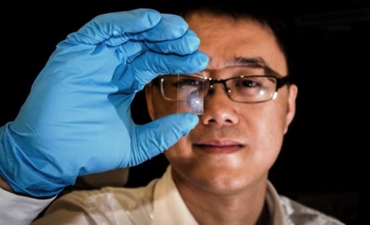
When mass-produced, graphene sensors are estimated to be at least five times less expensive as well. The new sensor may be the first to be able to detect broad-spectrum light, from the visible to mid-infrared, with high photo-response or sensitivity. This means it is suitable for use in all types of cameras, including infrared cameras, traffic speed cameras, and satellite imaging. Cameras fitted with the new sensor will soon be able to take clear and sharp photos in dim conditions. Wang said it is the first time that a broad-spectrum, high photosensitive sensor has been developed using pure graphene. His breakthrough, made by fabricating a graphene sheet into novel nano structures, was published this month in Nature Communications.
“We have shown that it is now possible to create cheap, sensitive, and flexible photo sensors from graphene alone. We expect our innovation will have great impact not only on the consumer imaging industry, but also in satellite imaging and communication industries, as well as the mid-infrared applications,” said Wang, who also holds a joint appointment in NTU’s School of Physical and Mathematical Sciences.
Graphene is a million times smaller than the thickest human hair—only one atom thick—and is made of pure carbon atoms arranged in a honeycomb structure. Known to have a high electrical conductivity, it also has other properties such as durability and flexibility. “While designing this sensor, we have kept current manufacturing practices in mind,” Wang said. “This means the industry can in principle continue producing camera sensors using the CMOS (complementary metal-oxide semiconductor) process, which is the prevailing technology used by the majority of factories in the electronics industry. Therefore, manufacturers can easily replace the current base material of photo sensors with our new nanostructured graphene material.
Wang had the idea to create nanostructures on graphene, which will “trap” light-generated electron particles for a much longer time, resulting in a much stronger electric signal. Such electric signals are processed into an image, such as a photograph captured by a digital camera. The “trapped electrons” technology is the key to achieving high photo-response in graphene, which makes it far more effective than the normal CMOS or CCD (charge-coupled device) image sensors, said Wang. Essentially, the stronger the electric signals generated, the clearer and sharper the photos.
“The performance of our graphene sensor can be further improved, such as the response speed, through nanostructure engineering of graphene, and preliminary results already verified the feasibility of our concept,” Wang said. This research, costing about $200,000, is funded by the Nanyang Assistant Professorship start-up grant and supported partially by the Ministry of Education Tier 2 and 3 research grants. Development of this sensor took Wang two years to complete. His team consisted of two research fellows, Dr. Zhang Yongzhe and Dr. Li Xiaohui, and four doctoral students. Wang has filed a patent through NTU’s Nanyang Innovation and Enterprise Office.
Our take
The next step is to work with the industry to develop the graphene sensor into a commercial product. That may not happen quickly. The integration of mono- and few-layer graphene and its functional derivatives into 3D macroscopic structures is an essential step to exploit the advanced properties of graphene sheets for practical applications, such as chemical filters, electrodes for energy storage device, or camera sensors.
Large-area ultrathin graphene films either are currently prepared by using catalytic pyrolysis of hydrocarbons at high temperatures (at around 1,000°C) or by using physical processes (e.g., vacuum filtration). The physical method is limited by its low efficiency, while the high-temperature method is unfeasible due to its cost and the difficultly in being directly integrated into the fabrication process for most electronics. However, in April, a team led by Xiaodong Chen, an assistant professor in the School of Materials Science and Engineering at NTU, demonstrated a fabrication method that could potentially form the precedent for industrial scale production of graphene materials.