The successor to Volta and Turing ushers in a new architecture.
Nvidia’s GPU Technology Conference in 2020 didn’t proceed like any before it. Originally scheduled for what turned out to coincide COVID-19 onslaught of March, Nvidia early on reworked the conference to an online event. And rather than scheduling talks and sessions live and packed over four days, the company metered them out over the course of several weeks.
However, in this case, Nvidia’s GPU deluge of disclosures and announcements wasn’t preceded by the biggest thunder clap but followed. After almost two months of weekly GTC session releases, parceling out research ideas, case studies, and tutorials covering topics that had already seen the light of day—Nvidia finally closed out the GTC 2020 stream in reverse, with CEO Jensen Huang’s keynote. Though an eventual introduction of Ampere was expected, its unveiling revealed quite a bit more than expected: a significantly enhanced architecture offering dramatic advancements in machine learning.
First, what looked exactly as expected: the roll-out strategy. As with Volta/Turing generations, Nvidia’s launch vehicle for the new generation was a big implementation, the A100 chip (if not max, call it Big Ampere) targeting the datacenter and optimized for machine learning, HPC, and cloud computing. Moving forward then, we’re likely looking at a family of Ampere derivatives, both GPGPU (for compute/datacenter) and graphics (gaming/workstations). Now, whether those appear as “Ampere” is another question, because when Volta appeared in graphics-focused GPU form, it became Turing. But semantics aside, Ampere (as Volta before it) will likely be leveraged in multi-pronged product lines across all Nvidia markets.
The A100 GPU
The Ampere flagship GPU, the A100, implements 54 billion transistors in a 7 nm chip using TSMC’s process. Nvidia credibly claims it is the largest 7 nm chip manufactured to date. Supporting the computation of all those transistors is stacked HBM2 memory, delivering up to 1.6 TB/s of peak memory bandwidth. (Bear in mind that focused on max performance and the datacenter, pricier HBM2 technology makes sense, but subsequent spins for mainstream GPUs—especially graphics focused—may adopt GDDR6 without the more expensive stacking.)
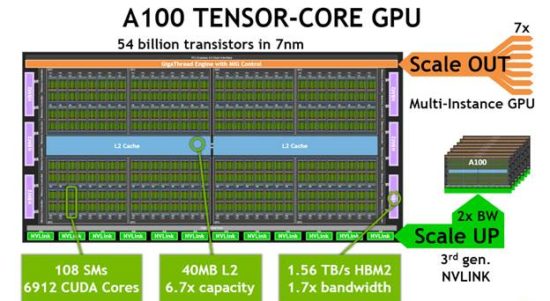
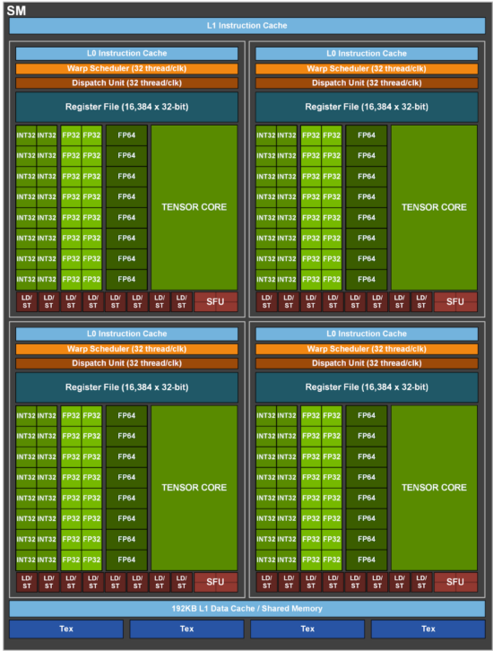
At 30,000 feet, Ampere follows the same basic Streaming Multiprocessor (SM) array architecture as its predecessors Turing, Volta, Pascal, Maxwell, and Kepler. Also like its predecessors, Ampere leveraged the larger transistor budget courtesy of the density shrink to deploy a bunch more Streaming Multiprocessors, 108 in total, for a total of 6912 CUDA cores, the long-time core atomic processing elements upon which the SMs and array are built.
But also like those predecessors, what sets Ampere apart is where Nvidia has focused its advancement efforts beyond scaling up the streaming multiprocessor array. The answer, at least for the flagship deep-learning and datacenter oriented A100, is in dramatically improving tensor compute performance and in scaling one physical GPU into a range of logical GPU sizes, from up to a datacenter-sized aggregation down to just a portion of a single physical GPU.
Specifically, Nvidia achieved those advances on five key technology fronts:
- The 3rd generation Tensor Core, dialing up both resources and features for much higher efficiency in deep-learning and HPC
- Supporting gains in execution throughput with balanced and commensurate data throughput
- The Elastic GPU, supporting both dramatically higher multi-GPU upscaling as well as sub-chip downscaling
Ampere’s Tensor Core: Volta’s on steroids
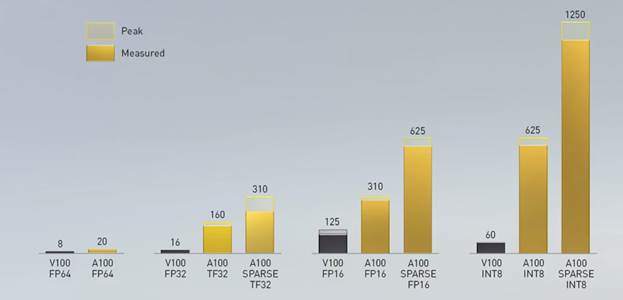
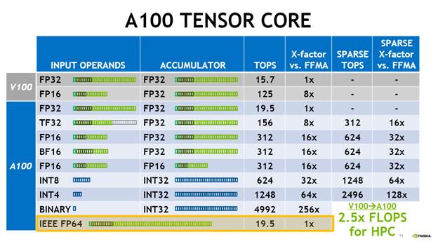
Volta’s big architectural splash came in the form of an integrated set of Tensor Cores for AI/ML. With Ampere, Nvidia doubled down, throwing both more resources and features to produce the A100 Tensor Core. In terms of raw throughput on existing tensor formats, the A100 boasts twice the TOPS mixed precision per SM of Volta (and then of course take into account the higher SM count for total peak speedup).
But more of the same tensor capabilities isn’t the bigger story of Ampere. Rather, it’s the combination of more resources combined with two new approaches: the TF32 tensor format and the exploitation of sparse matrices.
TF32: a newly crafted floating point format optimized for machine learning
Tensor Float32 is a new math mode in Nvidia’s A100 GPUs developed to handle the math in AI and HPC applications faster compared than single-precision floating-point math (FP32) on Volta GPUs. TF32 is a hybrid of half-precision 16-bit and single precision 32-bit float formats. TF32 running on Tensor Cores in A100 GPUs can provide up to 10× speedups compared to single precision floating-point math (FP32) on Volta GPUs and up to 20× faster than Volta when TF32 is combined with the structured sparsity on the A100.
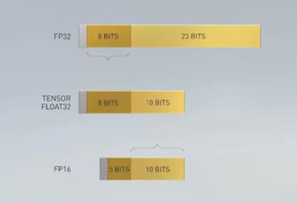
Of course, the whole point in making compromises of range and precision is to trim size, thereby reducing the load on interconnect, memory, datapath, and ALU widths. And that begs the question, why stick with the “32” in Tensor Float32? Well, that’s a bit misleading, in the sense that while it exceeds 16-bit width, it does not mean a full 32, but one extra sign bit more than the 18. Twenty bits would be an odd number for programmers to manipulate, but remember this is primarily (exclusively?) a format for intermediate calculations buried in the Tensor Cores. Programmers would still be able to work with FP32—and not have to bend over backward to cram into FP16—while the reduced-width Tensor Float32 provides for acceleration in implementation.
Reducing widths in implementation can be used to maintain performance while reducing silicon cost, or improve performance. With the A100, Nvidia not surprisingly chose the latter. Narrowing the width opens up space/transistors for more parallel computation, driving up throughput. Combining additional Tensor Core resources with TF32 support, Nvidia claims Ampere can process 10× the tensor arithmetic as Volta.
Neural networks on Ampere: creating sparsity to accelerate inference
And then there’s the third prong in Nvidia’s tensor compute performance upgrade for Ampere. Dovetailing with Tensor Float32 format is a technique Nvidia has formalized to retrain neural networks to a more efficient form, one that reduces unnecessary network computational density to create sparse networks more optimally executed in the Ampere architecture. Starting with a machine-trained DNN, algorithms prune network, tossing out accumulated zero value branches that in the final, trained network don’t contribute materially to the inference decisions.
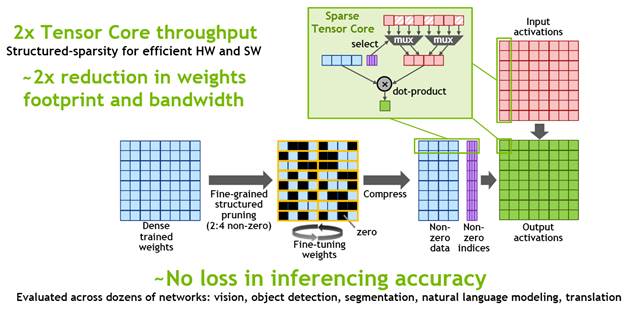
Naturally, eliminating zero value computation will speed up throughput, and given that Nvidia’s technique specifically retrains the network with half its weights removed, the sparsity re-training delivers around 2× faster inference. Nvidia-claimed 2× (presumably on average) with no loss in inference accuracy (based on its evaluation of “dozens of networks in vision, object detection, segmentation, natural language modeling and translation”).
All in all—combining more Tensor Core transistors, TF32, and leveraging intelligent sparsity—Nvidia claims an overall 20× speed-up (again, in common DNN types).
Dialing up data storage and movement to feed the beast
So with an order of magnitude (or more) faster tensor processing, clearly Ampere needed a boost in supporting data storage and movement infrastructure. Because without a means to feed the hungrier beast, all that new tensor horsepower would otherwise be wasted.
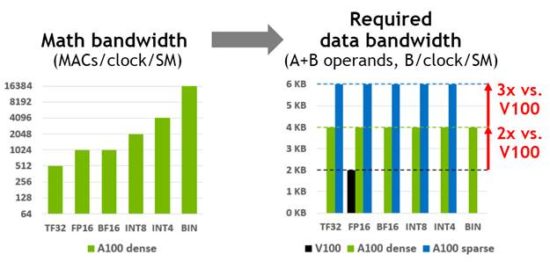
Toward the goal of dialing up the infrastructure in a balanced and commensurate fashion, Nvidia architects got their fingers into every level of the storage/memory hierarchy: register files, shared memory /L1 cache, L2, HBM2 DRAM and, ultimately, NVLink for inter-GPU data transport. Each stage was individually addressed to best match the demands of the new Tensor Core running critical neural network types. With respect to bandwidth, peak rates were driven up from 1.7 times to 3 times and for storage, from 1.3 times (DRAM) to 6.7 times (L2).
The Elastic GPU: 3rd Gen NVLink + Multi-instance GPU (MiG)
Borrowing an established term from the cloud, Nvidia introduced Elastic GPU technology in Ampere. Like its cloud namesake, the elastic refers the Ampere’s ability to scale both up and down, seamlessly and transparently to software. Just as cloud and virtually abstracted desktops are presented as logical instances of a component, rather than the physical component itself, a logical Ampere GPU presented to software can be comprised of a potentially large number of individual Ampere GPUs behind the curtain.
Leveraging 12 third-generation NVLink inter-GPU interconnect links—each doubled in performance from the Volta generation—a cluster of physical GPUs can be aggregated to create a datacenter-scale logical GPU. For example, the initial A100-based DGX A100 Ampere showcase computer (notably tapping AMD EPYC CPUs to host) comprises up to 56 physical A100 GPUs, yet presented as one monolithic GPU. Enabling the interconnect fabric is a new NVSwitch, with 36 ports running at 25 GB/s, per direction.
Multi-instance GPU
Scaling up by adding GPUs to create one bigger GPU that appears monolithic to the application. That’s great for big-to-unbounded compute problems. But Ampere supports the reverse as well with Multi-instance GPU (MiG) technology, breaking one physical GPU into multiple GPU instances, up to 7. Think of MiG as virtual GPU technology for deep-learning and compute applications, where each Ampere instance is allocated some amount of dedicated physical chip resource (e.g., L2 cache).
Both MiG and NVLink allow compute resource providers (e.g., both private and cloud) to more finely allocate GPU resources among clients and tasks. As such, an Amazon Web Services, for example, could right-size clients to logical slices of a single A100.
The Ampere is Nvidia’s chip for all seasons, at least this season. In his keynote kitchen speech, Jensen Huang stressed the Ampere scales from cars to the datacenter. Nvidia plans to be a major participant in the “smart everything revolution.” With new software, new architecture, the Mellanox interconnect technology and so much more, the company intends to participate on every level.