This next-generation compute platform will find a place in virtual reality, artificial intelligence, and deep learning as well as existing graphics-intensive applications.
By Alex Herrera
The veils are now officially off of Pascal, as Nvidia gave a complete rundown on the ins and outs of the company’s next-generation GPU, expected for production release in 2016. Delivering a dramatic step forward in compute and memory performance, Pascal is positioned not just as a showcase for existing bread-and-butter applications like gaming, but as an enabling platform for the spaces it wants to expand and profit from, like virtual reality (VR), deep learning, and artificial intelligence (AI).
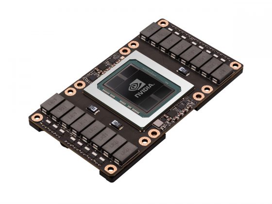
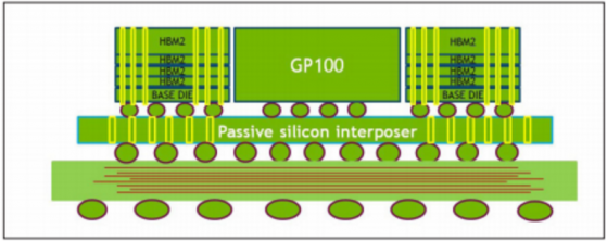
Nvidia’s first and flagship implementation of Pascal is the GP100 GPU, expected to ship first on a Tesla board in 2016 for HPC and supercomputing applications. As it did with all previous generations, Nvidia will most likely then release several subsequent derivatives of the GP100, with sizes, performance, and resources tuned to specific applications and market segments.
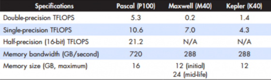
At a top level, Pascal offers impressive (albeit peak, best-case) throughput improvements over its predecessor, Maxwell. Nvidia says it has three times the compute performance, three times the memory bandwidth, and five times the GPU-to-GPU bandwidth (in multi-GPU environments). Those are hefty generation-to-generation boosts, but it’s worth putting them in context.
First, Nvidia’s triple jump in compute is a bit misleading, since they are comparing the GP100’s 20 TFLOPS performance with 16-bit precision (half precision) compared to Maxwell’s 7 TFLOPS with 32-bit precision (single precision). Now, applications that can accept the use of lower-precision half floats could see up to three times the throughput. But those relying primarily on single-precision (3D graphics rendering primarily) would see only about 50% better (maximum).
Comparing apples to apples, Pascal’s 9.6 TFLOPS single-precision max throughput means a more modest (though still quite respectable) double speed-up. On the other hand, the five times inter-GPU bump and three times memory boost are more direct comparisons, coming via the introduction of two long-awaited new technologies: high-speed GPU-to-GPU serial interconnect and stacked 3D memory (both addressed ahead).
The Pascal architecture
Architecturally, Pascal employs the same basic hierarchy of hardware structures that the company pioneered back in the Fermi days—most notably the atomic processing element, the CUDA core, and the primary processing engines built on a multitude of CUDA cores, the Stream Multiprocessor (SM).
Pascal’s SM groups CUDA processing cores, complementing the array with the processing units (e.g., rasterizers, instruction cache and schedulers, register file, texture units) needed to form a pipeline capable of executing threads of CUDA code. SM units are aggregated into Texture Processing Clusters (TPC), which are then further grouped to form Graphics Processing Clusters (GPC), which can handle the execution of complete CUDA “thread blocks.”
While tweaking names and the numbers of different structure, both of Pascal’s predecessors, Kepler and Maxwell, relied on the same basic hierarchical structure. Pascal followed suit, adding change that was to make Pascal’s SM half the size of Maxwell’s. Nvidia architects improved on Maxwell by splitting Maxwell’s 128-core SM in half to create two Pascal SMs. That may sound counter-intuitive, but in this case smaller is better. Fewer CUDA cores per SM means SMs can operate on a finer degree of code granularity, and a finer degree of granularity improves efficiency. The finer granularity, supported by faster and more plentiful storage, allows more CUDA cores to be utilized per cycle, on average.
Furthermore, although the SM gets smaller, the overall number of CUDA cores doesn’t shrink compared to Maxwell—rather, it grows. The GP100 chip has more than twice the SMs than Maxwell, and Nvidia padded each new SM with twice the supporting resources, including register file and shared memory.
All in all, the GP100 implementation has six GPCs, 30 TPCs, and 56 SMs for a total of 3840 CUDA cores and 240 texture units. The aggregate total of distributed on-chip memory cache grew 33% from 3072 KB to 4 MB.
Pascal’s most important architectural enhancements
Once the apple to the CPU orange, the GPU has steadily evolved to take on more and more CPU-type features. Once fixed-function hardwired accelerators, slaves to the CPU, the GPU is now highly programmable, supporting virtual memory supported by multilevel on-chip caches. Pascal continues that evolution, adding two more features that bring it another step closer to its CPU cousin: hardware page faulting and instruction-level preemption.
Nvidia has developed its virtual, unified memory incrementally over several generations. The basic construct of a unified GPU address space, combining three previously disparate GPU-only spaces into one contiguous map, appeared in Fermi back in 2010, greatly simplifying CUDA code compilation and enabling full C/C++ pointer support. Subsequent generations of Kepler and Maxwell extended on unified, virtual memory support, backed by extensions in CUDA, such that the CPU and GPU could now share a common unified address space.
With Pascal, Nvidia implemented two highly sought-after features to make more effective use of a shared virtual address space. The easier one (most likely) was to up the number of virtual address bits (to 49), allowing the shared space to encompass the typical 48-bit virtual address spaces of CPUs like Xeon, while accommodating the same amount of space for the GPU (or GPUs).
The more challenging feature was the implementation of hardware page faults. Without hardware page faults, Maxwell and previous generations required CUDA system software to synchronize accesses with the CPU prior to kicking off any CUDA kernel. Synchronization not only costs cycles to perform the communication, but potentially longer to wait for the sync. Now, with hardware page fault support, the GPU can start kernel execution without the pre-check and sync, and if a page is not resident in its local GPU memory, a page fault occurs and triggers a copy of that page from system memory to GPU memory. Code execution is simpler and faster.
Instruction-level preemption is another highly sought-after feature, particularly for compute-oriented programming. Previous GPUs had to complete kernel execution before getting on to other tasks, like rendering the screen or updating the GUI (graphical user interface). A long execution time could thus cause the machine to appear unresponsive until the kernel completed or the OS killed the process due to timeout. That made things harder on CUDA coders, who had to slice up work into smaller chunks on “unnatural” boundaries, just to avoid hangs and timeouts.
Instruction-level preemption changes all that. Working in very much the way it does on a CPU, preemption can now occur after completion of any instruction, and after the chip copies its context to GPU memory, can then proceed on another application or OS task. No more waiting for the full kernel to complete, and no more coding games to avoid time-outs.
Instruction-level preemption can help in interactive, visual applications as well, by limiting worst-case latency. Without it, not only can worst-case latency be longer, depending on code and data, but it’s not as deterministic, either. Both long and nondeterministic are bad when it comes to highly interactive uses of GPUs, two of which are very much in Nvidia’s gunsights moving forward. Remote graphics—as implemented by the company’s Grid line and targeting virtualized computing environments like VDI and cloud-hosted desktops—is one. And a recent high-profile addition to the company’s priority markets is virtual reality (VR). Experiences for both types of interactive computing rely on having the absolute lowest worst-case latencies possible. While architectures like Kepler and Maxwell made for quality interactive experiences for VDI, remote graphics, and VR, Pascal should do that much better.
NVLink a dramatic enabler for HPC performance
Last but not least of the major technology introductions in Pascal is NVLink. First previewed back in 2014, NVLink is Nvidia’s attempt to break the communication bandwidth bottleneck for multi-GPU systems. A high-speed serial interconnect, NVLink promises 160 GB/second of inter-chip communication, or what Nvidia claims as “5 to 12 times faster than the traditional PCIe Gen3 interconnect.”
Without NVLink, GPU-to-GPU communication had to pass through a PCIe switch. That topology not only offers substantially less total bandwidth, but it could block simultaneous GPU/GPU transfers that can now happen faster, and in parallel (at least in theory), via NVLink.
No doubt, builders of HPC and supercomputers will be overjoyed to see NVLink come to fruition. In fact, Nvidia’s primary partner in the world of supercomputers, IBM, is promising to integrate NVLink ports on its Power CPUs to speed not only GPU-to-GPU communication for Power-based HPC systems, but also direct CPU-to-GPU communication at speeds in excess of what is currently available with PCI Express.
NVLink should pay off for Nvidia in HPC and supercomputing markets; however, its appeal won’t extend much further. Not because it’s not a sensible solution to multi-GPU systems, but because there are simply not many markets that can stomach the added cost and added chip count and heat. The only corners of Nvidia’s traditional 3D graphics markets that currently take advantage of multiple GPUs are high-end gaming and high-end workstations, either for SLI acceleration or for multiple screens (though the latter need is increasingly handled with one GPU). As such, multi-GPU NVLink-enabled systems will, for all intents and purposes, be serving Tesla-focused HPC markets rather than Quadro- or Geforce-focused graphics markets.
What do we think?
It’s telling that Nvidia unveiled the GP100 version of Pascal with the Tesla brand, positioned for compute markets. The GP100 hundred will be a flagship GPU to deploy Pascal into high-end markets. But it won’t be the chip most customers in graphics markets like gaming or workstations will see. That chip (really will end up being several derivatives, as per the typical rollout) will share the same fundamental architecture, of course, but the implementation will be more optimized, trimming out costly features that don’t significantly benefit graphics.
Gone are the days when Nvidia would target compute and graphics markets with the same chip. The company learned that lesson back in 2010 with Fermi, when it created an all-in-one, kitchen-sink chip integrating all the features key to supporting both markets. The result was a chip that ran hot and was so big it cut into margins selling into its bread-and-butter graphics markets.
What is an example of extra hardware thrown in that chews up silicon space to support compute but not graphics? Well there are a few, but the big one is double precision (DP, or 64-bit floating point precision). It’s a must-have for certain HPC applications—and therefore a must for HPC installations—but it’s a don’t-care for virtually all 3D graphics applications. And it adds significant complexity and size.
What is an example of extra hardware thrown in that chews up silicon space to support compute but not graphics? Well there are a few, but the big one is double precision (DP, or 64-bit floating point precision). It’s a must-have for certain HPC applications—and therefore a must for HPC installations—but it’s a don’t-care for virtually all 3D graphics applications. And it adds significant complexity and size.
The sun has begun to set on Maxwell, and Pascal is quickly being readied as its replacement. By the end of 2016, it should have made a substantial mark—in one form or another—in all of Nvidia’s now-many GPU markets.