Beyond the block diagrams, FLOPS comparisons, and power requirements, the new system on a chip had to master complex human dynamics.
By Alex Herrera
[Editor’s Note: This article is excerpted from a longer report from the Hot Chips conference, as published in the current issue of Jon Peddie Research TechWatch.]
Technology conferences are usually a good place to get a read on industry trends, design shifts, and, every once in a while, a looming inflection point that stands to disrupt the status quo. For digital chip design, a favorite conference to scout remains Hot Chips. This year, Hot Chips provided a very clear picture of where chip vendors’ heads are at today: SoCs, low-power, and mobility.
The conference left us with a lot of the usual—block diagrams, FLOPS, bandwidths, and feature lists—as well as solid reaffirmation of where the emphasis in chip design remains. We also left with some serious thinking to do on how the semiconductor industry will have to adapt to remain viable in a future where its biggest weapon is no longer valid.
Today’s three hot design areas—systems on a chip (SoCs), power efficiency, and mobility— are interdependent; the first two are driven by the third. Whether talking conventional notebooks or the ever-emerging class of handhelds, reducing size and maximizing battery life are top priorities in many tech market segments, and they are the priorities in the hottest of those: tablets and smartphones. But mobile is not the only segment with new tech to brag about.
Xbox One silicon
Long awaited and recently unveiled, the Xbox One is Microsoft’s successor to the Xbox 360, introduced a long eight years ago. Because of the much shorter product cycles of their primary competition—gaming PCs—consoles need to shoot ahead of the curve. And the sheer magnitude of the main SoC Microsoft presented at Hot Chips shows that’s precisely where Microsoft was aiming.
Comprising the bulk of Xbox One’s functionality, the console’s Main SoC comes in at a hefty 363 mm2 in TSMC’s 28-nm HPM process, comprising 47 MB of storage and a total of 5 billion transistors. Yes, roughly five times the size of AMD’s Kabini (with a substantial chunk implementing the aforementioned 47 MB of on-chip SRAM). Though the sizes differ dramatically, Kabini and the AMD-co-engineered Xbox One SoC share plenty of the same DNA.
Xbox One processing comes courtesy of an octa-core AMD x86 CPU, an AMD Graphics Core Next (GCN) generation GPU, and 15 special-purpose processors. The latter processors save valuable CPU and GPU cycles by offloading simpler and well-understood processing to hardwired engines and DSPs—video encode and decode, audio, display, and several swizzle engines that (we assume) handle image copies unaligned in memory).
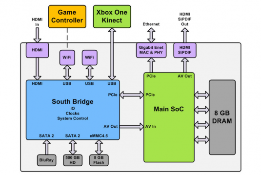
All internal processors access shared, unified memory via host/guest MMUs, allowing low-overhead co-processing by CPU and GPU (and other priority agents). Shared unified memory lets multiple processors working together pass pointers to data structures rather than copy the structure itself, which can be huge. But when big memory transfers are required, the SoC’s memory subsystem is up to the challenge, offering an impressive 200 GB/second of “realizable” bandwidth. Now, 30 to 68 GB/second of that bandwidth (depending on whether coherency is enforced) comes from external DRAM, while the bulk (204 GB/second peak) comes via 32 MB of embedded SRAM.
The CPU consists of eight Jaguar cores, the same core introduced in Kabini, and the GPU is a GCN (Southern Islands) class, DirectX 11.1+ engine, very similar to what’s in Kabini. Microsoft does say some “unique” functions for control processing were added, hence the “+” in DX 11.1+. Essentially, the SoC pairs two of Kabini’s 4-core clusters (complete with 2 MB 16-way L2). Xbox One’s GPU can transform and set up 1.71 Gprimitives/second, can shade with 1.31 TFLOPS, texture at 41 GTexels/second, and write/blend/color-convert 13.6 G Z-buffered pixels/second.
As with all these SoCs—and really any chip being built to do just about anything today—special care was made to minimize power consumption. Most notably, that means turning off big chunks of the chip when idle or not needed. Microsoft claims SoC clock gating can drop idle consumption to 2.5% of full power.
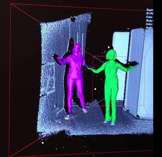
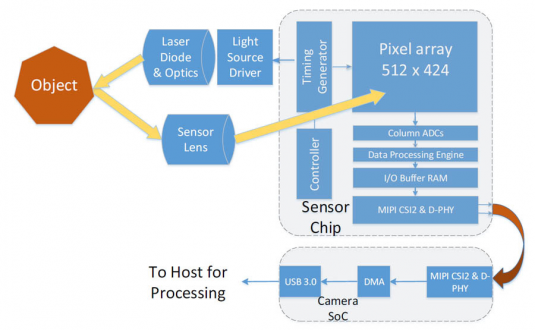
In a welcome respite from the otherwise dry (yet impressive!) Hot Chips disclosure, Microsoft talked about the techniques used by the new Kinect sensor chip coming with Xbox One. Including a 1080p camera optimized for low-light, Xbox One’s sensor chip was redesigned to improve gesture recognition to meet some stringent requirements. The chip needs to track gestures from players of various sizes, clothing, and distances from the console in real time. That implies a host of challenging tasks, for example, detecting and tracking a child’s 2-cm wrist at 4 meters from the camera while that child is playing with larger adults. Not easy.
Simply put, Kinect’s differential pixel sensor chip is detecting shapes and depth in the same way sonar works with sound. The sensor emits a modulated (square-ish) light signal, and based on how far out of phase that bounced return light is compared to the emitted signal, it can compute how far the shape is (light travels a centimeter in a few picoseconds). From there, by taking sums and differences of reflected signals, the chip can compute a grayscale view of the objects interacting in the field, independent of the ambient light in the scene.
And that’s just scratching the surface of the issues Kinect needs to resolve in real time. Consider also that two players may be wearing clothing of different reflectivity and located at different distances from the camera sensor. The farther away, the more the light attenuates, so the darker the player will be to the sensor. Similarly, the player with the white shirt will be much brighter than the one in dark. The result is an image with a tremendous range in intensity of approximately 2500x, demanding more complex and demanding HDR pixel storage and processing.
Alex Herrera is a senior analyst with Jon Peddie Research.


