A roundup of news from CPU manufacturers, courtesy of the Jon Peddie Research newsletter TechWatch.
[Editor’s Note: This is a roundup of reports from the most recent issue of TechWatch from Jon Peddie Research. For a free sample issue of TechWatch, visit the Jon Peddie Research website.]
Intel pushes Moore’s Law at 22 nanometers
The end of Moore’s law has been suggested and even forecast on and off for years, but almost everyone agreed that below 20 nm it was going to be dicey to try and maintain the concept of reducing transistor size. Short channel effects make it increasingly difficult to get the same amount of performance and energy efficiency improvements obtained in previous process transitions; there simply wouldn’t be enough atoms to get the transistor effect.
Several concepts have been proposed for extending Moore’s Law, but it’s been difficult to pick an obvious winner. The development process takes years and maybe a billion dollars for each idea, so no one can afford to try several at once and look for a winner. Intel, IBM, Global Foundries, and TSMC are all facing this issue, and making big, really gigantic bets in the process—and on a process.
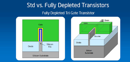
Intel began looking at these issues at the end of the last century and about that same time research papers were being published on FinFET—a 3D transistor with channels on the sides of a vertical fin structure. The principal advantage of the FinFET is that the wraparound gate gives excellent control— very high drive current when “on,”very low leakage when “off,” and very rapid switching between the two states.

The term FinFET was coined by three University of California, Berkeley researchers, Profs. Chenming Hu, Tsu-Jae King- Liu, and Jeffrey Bokor, to describe a non-planar, double-gate transistor built on an SOI substrate in 1999. Intel’s transistor also adds a third gate (on top) so Intel uses the term Tri-gate (or 3D). Intel is extending the transistor into the Z-axis, but the connections are still basically planar. It’s not that they are arranging transistors in three dimensions like stacking up sugar cubes (although that concept has been explored).
The basic concept of a FinFET or Tri-gate is shown in the accompanying diagram. Transistors have been designed in basically the same way since 1959. That was when Robert Noyce, Intel’s co-founder, and Jack Kilby of Texas Instruments independently developed the first integrated circuits. So for the past 60 years we’ve been making transistors basically the same way; creating source, drain and channel regions in the silicon substrate, then depositing the gate dielectric, then forming the gate electrode. Now it’s time to grow up.
By adding more surface area for the transistor’s gate the threshold voltage for the gate can be reduced. That in turn makes the slope from the no-current flow state to the full-current flow state steeper—and steeper means faster. To build these finned transistors Intel will use immersion lithography with some double patterning, and will include gate last high-K metal gates and strained silicon—in other words all the tricks of the trade today. But the finned transistor marks the end of planar—Intel’s last planar transistor was built using a 32 nm process.
As exciting and interesting as this transistor design is, make no mistake— it’s not a laboratory curiosity—these new finned transistors at 22 nm are being built and sampled now and will be in full production by the end of 2011. That puts Intel a node and process ahead of all the competition. When Intel first started hinting about finFETs and 22 nm the general feeling in the industry was maybe sometime in 2012, even though Intel had pretty much been hitting the two year cadence for some time. After all, this was new territory and you don’t commit three, four, or five giant multi-billion dollar fabs to a science project—it’s got to work and be bullet proof—in other words, it has to produce high yields.
Intel beat their own time schedule; needless to say there’ll be some nice bonus checks this year.
This is Intel’s game. The only way the company can command higher sales price for its chips, and the delightful margins they earn from them, is to have killer differentiation and competitive advantages. And they get it first and foremost by making the best transistors in the world in humongous quantities—and if they succeed in the mobile space the quantities get even larger.
What about mobile? Obviously Intel will bring 22 nm to their Atom and SoC product lines; but when? The “future” is not the same for all parts. This year is the “future” for PCs, the second half to be exact. And although Intel did not say specifically when they would have Atom in 22 nm, the feeling is next year. Given the obvious advantage a 22 nm transistor seems to offer in lower power consumption and higher speeds, Sphinx-like Intel has befuddled the analysts, pundits, and OEMs with the delay. Clearly there are factors at work in getting 22 nm to be useful in nano-like micro-mobile parts that are not obvious to those outside Intel’s fabulous fabs. Be patient grasshopper, in time you will learn.
The upcoming processor lineup extends all the way up to the top in the HPC space including the Knights Corner co-processor. Intel says when the transistors are used in the ultra-mobile space they will bring a 37% performance increase at low voltage and >50% power reduction at constant performance—how’s that for following Moore’s Law?
New VIA Technologies QuadCore CPU; so many bits in such a small package
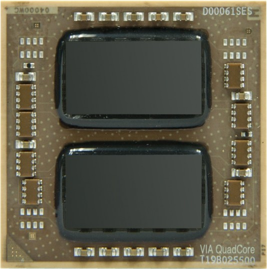
VIA Technologies introduces a multichip quadcore processor, claiming it is the lowest power quadcore processor on the market. Claiming a Thermal Design Power (TDP) rating of only 27.5 watts, VIA says the 1.2+ GHz VIA QuadCore processor is 21% more energy efficient than competitors such as the AMD Brazos, operating at 35 watts.

VIA QuadCore combines Intel’s data center roadmap for 22 nm, with four VIA Nano cores on two dies, offering enhanced multi-tasking and superb multimedia performance on a low power budget. The VIA Nano (formerly code named VIA Isaiah) is a 64-bit CPU with support for features like the x86-64 instruction set and x86 virtualization, and was released in 2008 after five years of development by the Centaur CPU division in Austin. The processor has a number of VIA-specific x86 extensions designed to boost efficiency in low-power appliances.
Initially available at a speed of 1.2+GHz, VIA QuadCore processors are 64-bit compatible and feature Adaptive Overclocking, 4MB L2 cache, and a 1333MHz V4 (FS) Bus. VIA says the processor has high-performance superscalar processing, out-of-order x86 architecture, an efficient floating point unit (2 clock SP multiplies), hardware virtualization support, power and thermal management, AES hardware security features, and secure Hash Algorithm: SHA-1, SHA-256, SHA-384, SHA-512.
Other advanced features include VIA VT virtualization, a technology that allows legacy software and applications to be used in virtual scenarios without impacting performance, and VIA Pad-Lock with the Advanced Cryptography Engine, which delivers fast AES encryption. This hardware-based security feature offers data encryption on the fly, an essential tool in content protection and system security.
The processor will be teamed up with either VIA’s VX900, a DirectX 9 IGP with integrated north and south bridge, or the VN1000, a DirectX 10.1 chipset which includes Display Port and HDMI support as well as options for dual and single channel LVDS, DVI and VGA outputs. Next quarter the company will introduce a DirectX 11 chipset.
The new chip is targeted at desktop PCs, notebooks, small form factor PCs, and mini-server system design applications.
VIA has contented itself with batting clean up. Its QuadCore comes late, but according to benchmark tests published online, it performs competitively against the low power processors from Intel and AMD. VIA isn’t pushing any barriers here. What VIA is calling a Quadcore is two dual-core chips with their own caches communicating through a 1333 MHz front side bus. VIA has graphics thanks to its partner S3 but we’re thinking that we won’t be seeing integrated graphics in the processors for some time given how long it’s taken the company to catch up with a Quadcore. VIA’s processors are designed in Austin by the Centaur team. These guys seem to have their own timetables, and after all Taiwan is so very, very far away.
AMD back in the game with Phenom
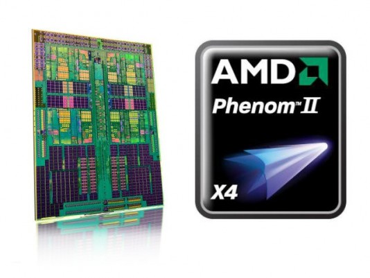
AMD has added its fastest quadcore processor to the AMD Phenom II desktop processor family, the AMD Phenom II X4 980 Black Edition processor. The AMD Phenom II X4 980 Black Edition processor is unlocked, which enables gamers and PC enthusiasts to overclock and optimize total system performance. This quad-core processor operates at 3.7GHz with 6MB of L3 cache and a TDP of 125W and sells for $185.

If clock speed is the primary measure of a CPU’s performance then AMD wins. Intel’s top of the line Core i7 2600 runs at 3.43 GHz and sells for $294. However, Intel’s processor offers TurboBoost which boosts the clock of a single core up to 3.8 GHz.
We haven’t gotten an X4 980 yet so can’t give you any performance comparisons right now. AMD was the processor of choice for gamers a few years back, but when Intel brought out the Westmere line Intel took the crown.
AMD’s problems with the Barcelona processor slowed its comeback. AMD has been nibbling away at Intel’s market share, on the low end with Fusion and the high end with Bulldozer. It could continue to nibble if the X4 980 shows well.


